|
|
|
|
|
|
 |
 |
| Full Custom Layout |
|
| The analog IP development and custom layout service needed by the customer, the LPE TEG design service to extract the parasitic, electric, and spice model parameter, the machine material performance evaluation TP design service to check the physical characteristics of equipment and materials, and the CAD design and GDS conversion service for the compatibility among EDA tools are supported.
Furthermore, The mask tooling and the FAB service are provided to have the finally finished chip directly enter the market without the involvement in the FAB process by the customer. |
|
| |
 |
|
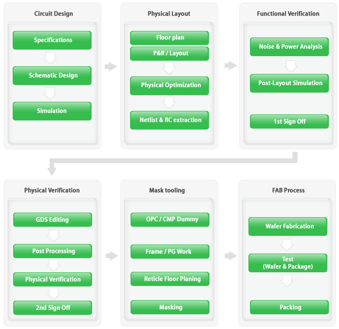
It supports the whole process from the circuit design to the FAB service as the analog & mixed mode customer layout service, or the service for each stage wanted by the customer can be rendered.
 Circuit Design : The verification stage thorugh the schematic design and simulation when deciding the specification Circuit Design : The verification stage thorugh the schematic design and simulation when deciding the specification
Physical Layout : The stage of creating the design drawing of the physical layer and extracting the netlist and
parasite ingredients
Functional Verification : The stage to add the parasite ingredients to the netlist extracted from the physical layout
to check the integrity of the action due to changes in circumstances
Physical Verification : Checking if the physical layer design with the verified integrity is suitable to the process
specification
Mask tooling : The pre-stage needed for manufacturing the mask such as dummy generation, frame/PG work, etc.
Fabrication : Guaranteeing the quality of customer products through various package supports such as high pin
count, very small & thin packaging and the experience in verified production process and quality control after
handling the FAB process |
|
| |
 |
|
 |
| |
|
| |
|
|
|
|
|